
Let and be two vectors. The value of the coefficient in the expression , which minimizes the length of the error vector , is


Explanation Locked!
Unlock this branch to view the explanation, track, bookmark and more.
Sign in to UnlockThe rate of increase, of a scalar field in the direction at a point is


2
4
Explanation Locked!
Unlock this branch to view the explanation, track, bookmark and more.
Sign in to UnlockLet . Which of the following cannot be a value of ?


Explanation Locked!
Unlock this branch to view the explanation, track, bookmark and more.
Sign in to UnlockThe value of the contour integral,
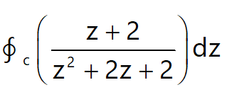 , where the contour is

, taken in the counter clockwise direction, is


Explanation Locked!
Unlock this branch to view the explanation, track, bookmark and more.
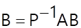
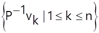
Sign in to UnlockLet the sets of eigenvalues and eigenvectors of a matrix be and , respectively. For any invertible matrix , the sets of eigenvalues and eigenvectors of the matrix , where , respectively, are

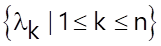
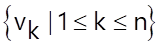


and
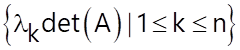
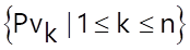
and
and
and
Explanation Locked!
Unlock this branch to view the explanation, track, bookmark and more.
Sign in to UnlockIn a semiconductor, if the Fermi energy level lies in the conduction band, then the semiconductor is known as
degenerate -type.

degenerate -type.

non-degenerate -type.
non-degenerate -type.
Explanation Locked!
Unlock this branch to view the explanation, track, bookmark and more.
Sign in to UnlockFor an intrinsic semiconductor at temperature , which of the following statement is true?

Explanation Locked!
Unlock this branch to view the explanation, track, bookmark and more.
Sign in to UnlockA series RLC circuit has a quality factor of 1000 at a center frequency of . The possible values of and are


and


and

and

and

Explanation Locked!
Unlock this branch to view the explanation, track, bookmark and more.
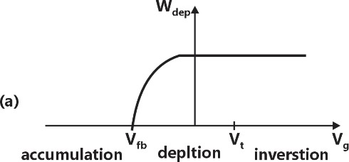
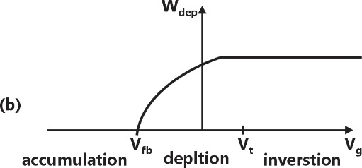
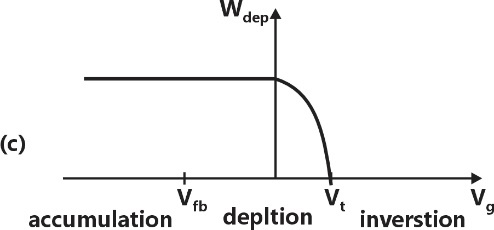
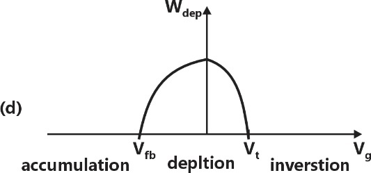
Sign in to UnlockFor a MOS capacitor, and are the flat-band voltage and the threshold voltage, respectively. The variation of the depletion width for varying gate voltage is best represented by


Explanation Locked!
Unlock this branch to view the explanation, track, bookmark and more.
Sign in to UnlockConsider a narrow band signal, propagating in a lossless dielectric medium , with phase velocity and group velocity . Which of the following statement is true?


( is the velocity of light in vacuum.)


Explanation Locked!
Unlock this branch to view the explanation, track, bookmark and more.
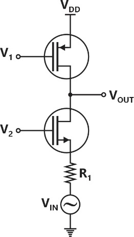
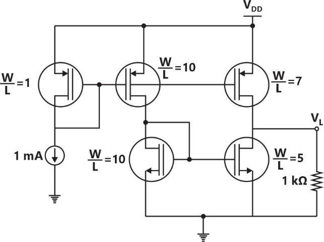
Sign in to UnlockIn the circuit shown below, and are bias voltages. Based on input and output impedances, the circuit behaves as a


Explanation Locked!
Unlock this branch to view the explanation, track, bookmark and more.
Sign in to UnlockA cascade of common-source amplifiers in a unity gain feedback configuration oscillates when
the closed loop gain is less than 1 and the phase shift is less than .

the closed loop gain is greater than 1 and the phase shift is less than .
the closed loop gain is less than 1 and the phase shift is greater than .
the closed loop gain is greater than 1 and the phase shift is greater than .
Explanation Locked!
Unlock this branch to view the explanation, track, bookmark and more.
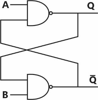
Sign in to UnlockIn the circuit shown below, and are the inputs. The logical function realized by the circuit shown below is

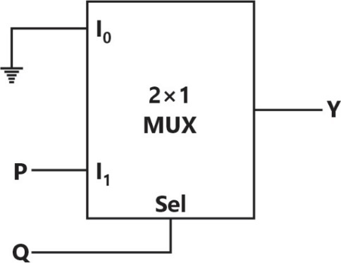


Explanation Locked!
Unlock this branch to view the explanation, track, bookmark and more.
Sign in to UnlockThe synchronous sequential circuit shown below works at a clock frequency of . The throughput, in bits/s, and the latency, in ns, respectively, are


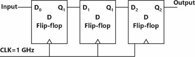
1000,3

2000,3

Explanation Locked!
Unlock this branch to view the explanation, track, bookmark and more.
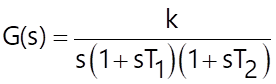
Sign in to UnlockThe open loop transfer function of a unity negative feedback system is , where and are positive constants. The phase cross-over frequency, in rad/s, is


Explanation Locked!
Unlock this branch to view the explanation, track, bookmark and more.
Sign in to UnlockConsider a system with input and output . The system is


Explanation Locked!
Unlock this branch to view the explanation, track, bookmark and more.
Sign in to UnlockLet be a strictly band-limited signal M bandwidth B and energy E. Assuming the energy in the signal is


E
2E
Explanation Locked!
Unlock this branch to view the explanation, track, bookmark and more.
Sign in to UnlockThe Fourier transform of is


Note:


Explanation Locked!
Unlock this branch to view the explanation, track, bookmark and more.
Sign in to UnlockIn the table shown below, match the signal type with its spectral characteristics.
Signal Type
(i) Continuous, aperiodic
(ii) Continuous, periodic
(iii) Discrete, aperiodic
(iv) Discrete, periodic
Spectral Characteristics
(a) Continuous, aperiodic
(b) Continuous, periodic
(c) Discrete, aperiodic
(d) Discrete, periodic
(i) (a), (ii) (b), (iii) (c), (iv) (d)

(i) (a), (ii) (c), (iii) (b), (iv) (d)
(i) (d), (ii) (b), (iii) (c), (iv) (a)
(i) (a), (ii) (c), (iii) (d), (iv) (b)
Explanation Locked!
Unlock this branch to view the explanation, track, bookmark and more.
Sign in to UnlockThe signal-to-noise ratio (SNR) of an ADC with a full-scale sinusoidal input is given to be 61.96 . The resolution of the ADC is __________ (rounded off to the nearest integer). bits.

Explanation Locked!
Unlock this branch to view the explanation, track, bookmark and more.
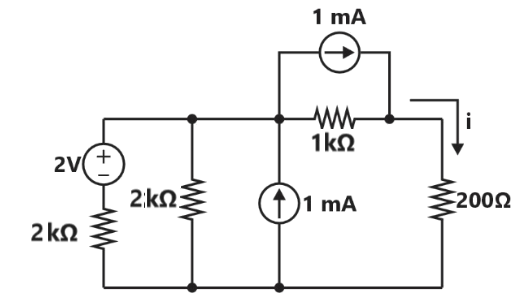
Sign in to UnlockIn the circuit shown below, the current I flowing through 200 Ω resistor is ________ mA.
(rounded off to two decimal places).
Explanation Locked!
Unlock this branch to view the explanation, track, bookmark and more.
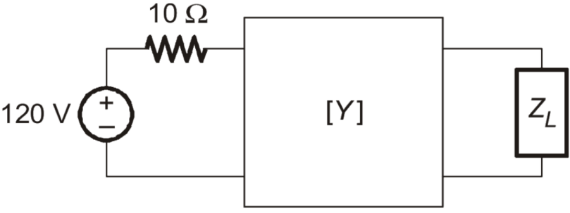
Sign in to UnlockFor the two port network shown below, the [Y]-parameters is given as

The value of load impedance , in , for maximum power transfer will be _________.


(rounded off to the nearest integer).
Explanation Locked!
Unlock this branch to view the explanation, track, bookmark and more.
Sign in to UnlockFor the circuit shown below, the propagation delay of each NAND gate is . The critical path delay, in ns, is ________ (rounded off to the nearest integer).

Explanation Locked!
Unlock this branch to view the explanation, track, bookmark and more.
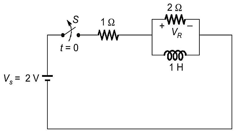
Sign in to UnlockIn the circuit shown below, switch S was closed for a long time. If the switch is opened at t=0, the maximum magnitude of the voltage in volts, is ________ (rounded off to the nearest integer).

Explanation Locked!
Unlock this branch to view the explanation, track, bookmark and more.
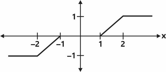
Sign in to UnlockA random variable , distributed normally as , undergoes the transformation , given in the figure. The form of the probability density function of is (In the options given below, are non-zero constants and is piecewise continuous function)


Explanation Locked!
Unlock this branch to view the explanation, track, bookmark and more.
Sign in to UnlockThe value of the line integral along the straight line joining the points and is


Explanation Locked!
Unlock this branch to view the explanation, track, bookmark and more.
Sign in to UnlockLet be an real column vector with length . The trace of the matrix is


Explanation Locked!
Unlock this branch to view the explanation, track, bookmark and more.
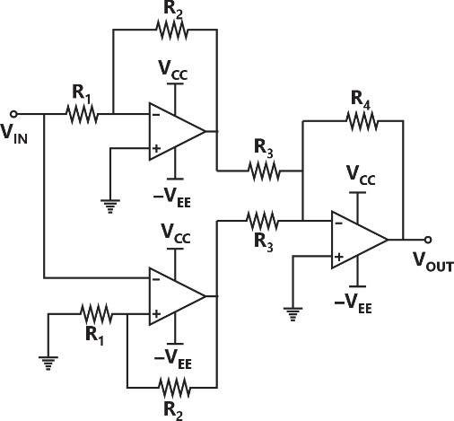
Sign in to UnlockThe of the circuit shown below is


Explanation Locked!
Unlock this branch to view the explanation, track, bookmark and more.
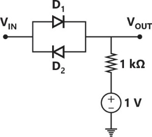
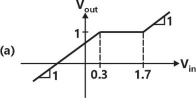
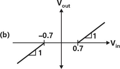
Sign in to UnlockIn the circuit shown below, and are silicon diodes with cut-in voltage of . and are input and output voltages in volts. The transfer characteristic is


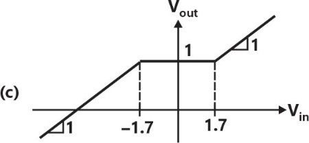
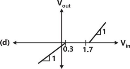
Explanation Locked!
Unlock this branch to view the explanation, track, bookmark and more.
Sign in to UnlockA closed loop system is shown in the figure where and . The steady state error due to a ramp input is given by


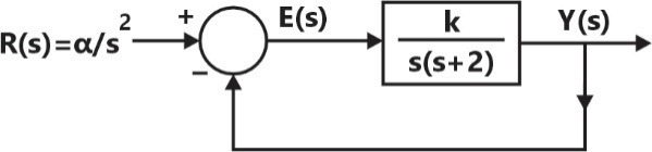


Explanation Locked!
Unlock this branch to view the explanation, track, bookmark and more.
Sign in to UnlockIn the following block diagram, and are two inputs. The output is expressed as


. and are given by


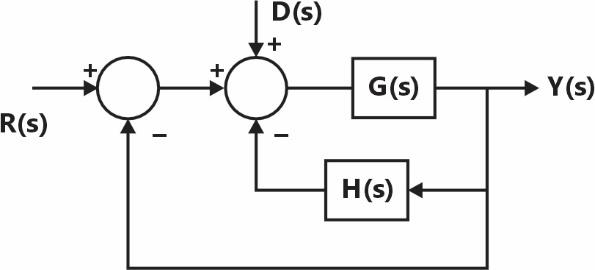
and


and


and
and
Explanation Locked!
Unlock this branch to view the explanation, track, bookmark and more.
Sign in to UnlockThe state equation of a second order system is is the initial condition.

Suppose and are two distinct eigenvalues of A and and are the corresponding eigenvectors. For constants and , the solution, , of the state equation is


Explanation Locked!
Unlock this branch to view the explanation, track, bookmark and more.
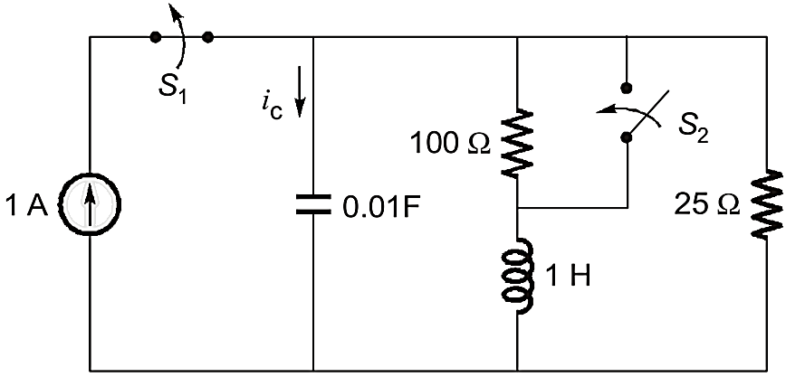
Sign in to UnlockThe switch was closed and was open for a long time. At , switch is opened and is closed, simultaneously. The value of , in amperes, is


Explanation Locked!
Unlock this branch to view the explanation, track, bookmark and more.
Sign in to UnlockLet a frequency modulated (FM) signal , where is a message signal of bandwidth . It is passed through a non-linear system with output . Let denote the FM bandwidth. The minimum value of required to recover from is


Explanation Locked!
Unlock this branch to view the explanation, track, bookmark and more.
Sign in to UnlockThe h-parameters of a two port network are shown below. The condition for the maximum small signal voltage gain is

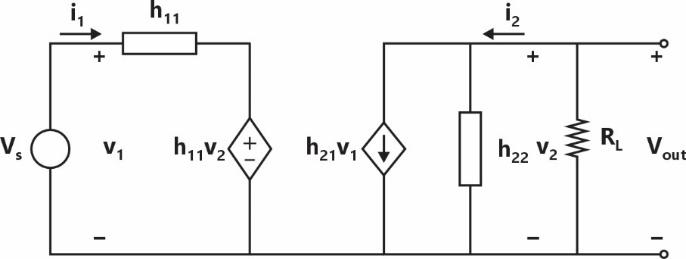
very high and


very high, very high and


very high, very high and


very high and very high

Explanation Locked!
Unlock this branch to view the explanation, track, bookmark and more.
Sign in to UnlockConsider a discrete-time periodic signal with period . Let the discrete-time Fourier series (DTFS) representation be , where


and . The value of the sum is


Explanation Locked!
Unlock this branch to view the explanation, track, bookmark and more.
Sign in to UnlockLet an input having discrete time Fourier transform.

be passed through an LTI system. The frequency response of the LTI system is . The output of the system is


Explanation Locked!
Unlock this branch to view the explanation, track, bookmark and more.
Sign in to UnlockLet be passed through an LTI system having impulse response . The output of the system is


Explanation Locked!
Unlock this branch to view the explanation, track, bookmark and more.
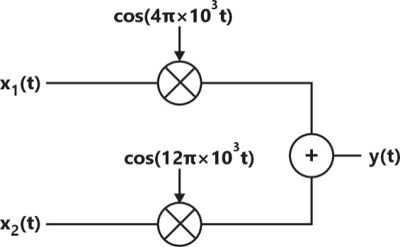
Sign in to UnlockLet and be two band-limited signals having bandwidth each. In the figure below, the Nyquist sampling frequency, in , required to sample , is


Explanation Locked!
Unlock this branch to view the explanation, track, bookmark and more.
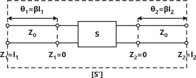
Sign in to UnlockThe S-parameters of a two port network is given as

with reference to . Two lossless transmission line sections of electrical lengths and are added to the input and output ports for measurement purposes, respectively. The Sparameters of the resultant two port network is


Explanation Locked!
Unlock this branch to view the explanation, track, bookmark and more.
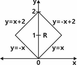
Sign in to UnlockThe value of the integral over the region , given in the figure, is __________(rounded off to the nearest integer).


Explanation Locked!
Unlock this branch to view the explanation, track, bookmark and more.
Sign in to UnlockIn an extrinsic semiconductor, the hole concentration is given to be where is the intrinsic carrier concentration of . The ratio of electron to hole mobility for equal hole and electron drift current is given as _________(rounded off to two decimal places).


Explanation Locked!
Unlock this branch to view the explanation, track, bookmark and more.
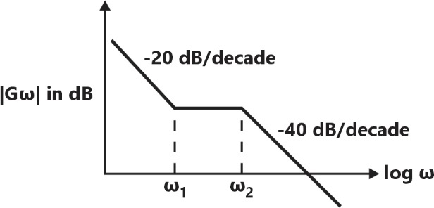
Sign in to UnlockThe asymptotic magnitude Bode plot of a minimum phase system is shown in the figure. The transfer function of the system is , where and c are positive constants. The value of is __________. (rounded off to the nearest integer).


Explanation Locked!
Unlock this branch to view the explanation, track, bookmark and more.
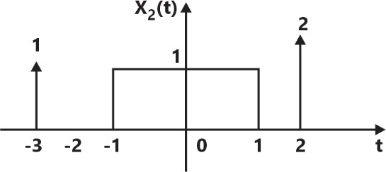
Sign in to UnlockLet and is shown in the figure below. For , the is _________. (rounded off to the nearest integer).


Explanation Locked!
Unlock this branch to view the explanation, track, bookmark and more.
Sign in to UnlockLet be a white Gaussian noise with power spectral density . If is input to an LTI system with impulse response . The average power of the system output is __________ W. (Rounded off to two decimal place).


Explanation Locked!
Unlock this branch to view the explanation, track, bookmark and more.
Sign in to UnlockA transparent dielectric coating is applied to glass to eliminate the reflection of red light . The minimum thickness of the dielectric coating, in , that can be used is ________. (rounded off to two decimal places).


Explanation Locked!
Unlock this branch to view the explanation, track, bookmark and more.
Sign in to UnlockIn a semiconductor device, the Fermi-energy level is above the valence band energy. The effective density of states in the valence band at is . The thermal equilibrium hole concentration in silicon at is _________. (rounded off to two decimal places). Given KT at is .


Explanation Locked!
Unlock this branch to view the explanation, track, bookmark and more.
Sign in to UnlockA sample and hold circuit is implemented using a resistive switch and a capacitor with a time constant of . The time for sampling switch to stay closed to charge a capacitor adequately to full scale voltage of with 12-bit accuracy is ________ .


(rounded off to two decimal places)
Explanation Locked!
Unlock this branch to view the explanation, track, bookmark and more.
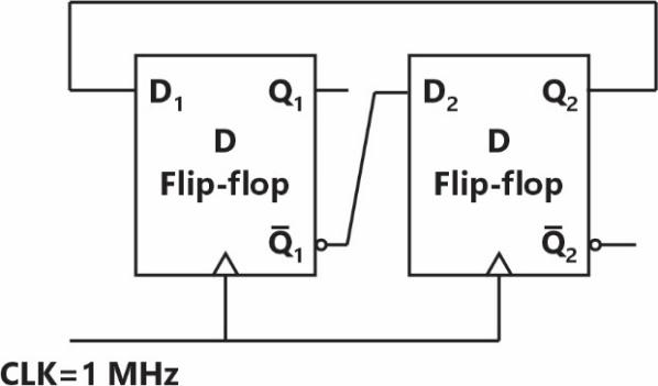
Sign in to UnlockIn a given sequential circuit, initial states are and . For a clock frequency of , the frequency of signal in , is ________. (rounded off to the nearest integer).


Explanation Locked!
Unlock this branch to view the explanation, track, bookmark and more.
Sign in to UnlockIn the circuit below, the voltage is _______V. (rounded off to two decimal places)

Explanation Locked!
Unlock this branch to view the explanation, track, bookmark and more.
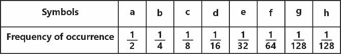
Sign in to UnlockThe frequency of occurrence of 8 symbols (a-h) is shown in the table below. A symbol is chosen and it is determined by asking a series of "yes/no" questions which are assumed to be truthfully answered. The average number of questions when asked in the most efficient sequence, to determine the chosen symbol, is _______ (rounded off to two decimal places).
Explanation Locked!
Unlock this branch to view the explanation, track, bookmark and more.
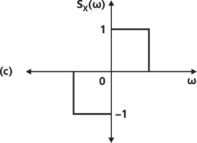
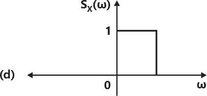
Sign in to UnlockFor a real signal, which of the following is/are valid power spectral density/densities?


Explanation Locked!
Unlock this branch to view the explanation, track, bookmark and more.
Sign in to UnlockThe standing wave ratio on a lossless transmission line terminated in an unknown load impedance is found to be 2.0. The distance between successive voltage minima is 30 cm and the first minimum is located at 10 cm from the load. can be replaced by an equivalent length and terminating resistance of the same line. The value of and , respectively, are


Explanation Locked!
Unlock this branch to view the explanation, track, bookmark and more.
Sign in to UnlockThe electric field of a plane electromagnetic wave is

Which of the following combination(s) will give rise to a left handed elliptically polarized (LHEP) wave?


Explanation Locked!
Unlock this branch to view the explanation, track, bookmark and more.
Sign in to UnlockThe following circuit(s) representing a lumped element equivalent of an infinitesimal section of a transmission line is/are
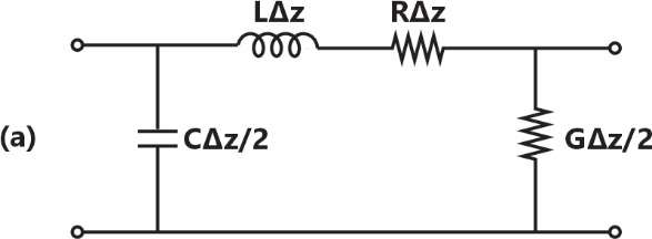
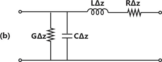
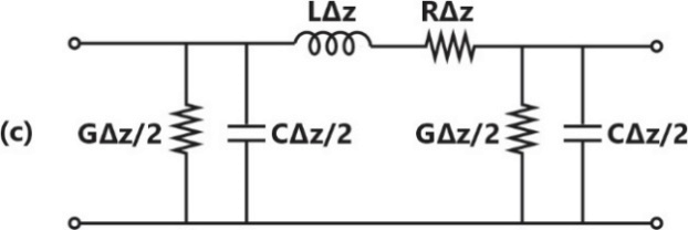
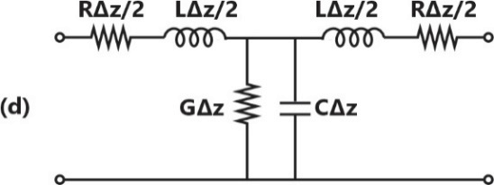
Explanation Locked!
Unlock this branch to view the explanation, track, bookmark and more.
Sign in to Unlock