Electronic Devices
Semiconductor Physics
Practice questions from Semiconductor Physics.
10
Total0
Attempted0
Correct0
IncorrectWhich of the following can be used as an n-type dopant for silicon?
Select the correct option(s).
Explanation Locked!
Unlock this branch to view the explanation, track, bookmark and more.
Sign in to UnlockThe intrinsic carrier concentration of a semiconductor is at 300 K.

If the electron and hole mobilities are and , respectively, then the intrinsic resistivity of the semiconductor (in ) at 300 K is _________.


(Charge of an electron .)

Explanation Locked!
Unlock this branch to view the explanation, track, bookmark and more.
Sign in to UnlockThe electron mobility in a non-degenerate germanium semiconductor at 300 K is .


The electron diffusivity at 300 K (in , rounded off to the nearest integer) is _________.


(Consider the Boltzmann constant and the charge of an electron .)

Explanation Locked!
Unlock this branch to view the explanation, track, bookmark and more.
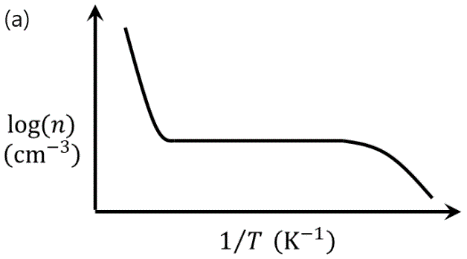
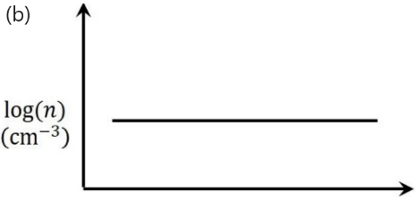
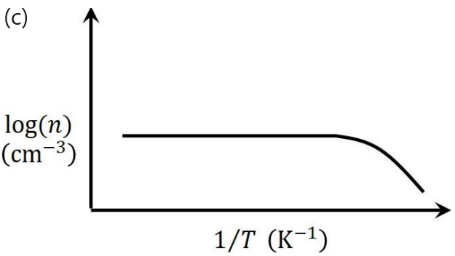
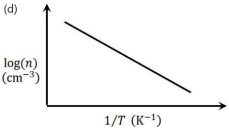
Sign in to UnlockFor non-degenerately doped n-type silicon, which one of the following plots represents the temperature (𝑇) dependence of free electron concentration (𝑛)
Explanation Locked!
Unlock this branch to view the explanation, track, bookmark and more.
Sign in to UnlockA non-degenerate n-type semiconductor has neutral dopant atoms. Its Fermi level is located at below the conduction band and the donor energy level has a degeneracy of 2. Assuming the thermal voltage to be . The difference between and (in , rounded off to two decimal places) is __________.


Explanation Locked!
Unlock this branch to view the explanation, track, bookmark and more.
Sign in to UnlockThe free electron concentration profile in a doped semiconductor at equilibrium is shown in the figure, where the points , and mark three different positions. Which of the following statements is/are true?


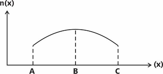
For between B and C, the electron diffusion current is directed from to .


For between B and A, the electron drift current is directed from B to A.
For between B and C, the electric field is directed from B to C.
For between B and A, the electric field is directed from to .

Explanation Locked!
Unlock this branch to view the explanation, track, bookmark and more.
Sign in to UnlockIn a semiconductor, if the Fermi energy level lies in the conduction band, then the semiconductor is known as
degenerate -type.

degenerate -type.

non-degenerate -type.
non-degenerate -type.
Explanation Locked!
Unlock this branch to view the explanation, track, bookmark and more.
Sign in to UnlockFor an intrinsic semiconductor at temperature , which of the following statement is true?

Explanation Locked!
Unlock this branch to view the explanation, track, bookmark and more.
Sign in to UnlockIn an extrinsic semiconductor, the hole concentration is given to be where is the intrinsic carrier concentration of . The ratio of electron to hole mobility for equal hole and electron drift current is given as _________(rounded off to two decimal places).


Explanation Locked!
Unlock this branch to view the explanation, track, bookmark and more.
Sign in to UnlockIn a semiconductor device, the Fermi-energy level is above the valence band energy. The effective density of states in the valence band at is . The thermal equilibrium hole concentration in silicon at is _________. (rounded off to two decimal places). Given KT at is .


Explanation Locked!
Unlock this branch to view the explanation, track, bookmark and more.
Sign in to Unlock