Digital Electronics
Microprocessor
Practice questions from Microprocessor.
33
Total0
Attempted0
Correct0
IncorrectIn a given 8-bit general purpose micro-controller there are following flags. C-Carry, A-Auxiliary Carry, O-Overflow flag, P-Parity (0 for even, 1 for odd) and are the two general purpose registers of the micro-controller. After execution of the following instructions, the decimal equivalent of the binary sequence of the flag pattern [CAOP] will be


MOV RO,

MOV R1, +0x46
ADD R0, R1
Explanation Locked!
Unlock this branch to view the explanation, track, bookmark and more.
Sign in to UnlockAn 8085 microprocessor accesses two memory locations (2001H) and (2002H), that contain 8-bit numbers 98H and B1H, respectively. The following program is executed:
LXI H,2001H
MVI A, 21H
INXH
ADD M
INXH
MOV M, A
HLT
At the end of this program, the memory location 2003H contains the number in decimal (base 10) form.
Explanation Locked!
Unlock this branch to view the explanation, track, bookmark and more.
Sign in to UnlockAn output device is interfaced with 8–bit microprocessor 8085A. The interfacing circuit is shown in figure

The interfacing circuit makes use of 3 Line to 8 Line decoder having 3 enable lines . The address of the device is


Explanation Locked!
Unlock this branch to view the explanation, track, bookmark and more.
Sign in to UnlockIn an 8085 microprocessor, the following program is executed
Address location – Instruction
2000H XRA A
2001H MVI B, 04H
2003H MVI A, 03H
2005H RAR
2006H DCR B
2007H JNZ 2005
200AH HLT
At the end of program, register A contains
Explanation Locked!
Unlock this branch to view the explanation, track, bookmark and more.
Sign in to UnlockIn 8085A microprocessor, the operation performed by the instruction LHLD is


Explanation Locked!
Unlock this branch to view the explanation, track, bookmark and more.
Sign in to UnlockA portion of the main program to call a subroutine SUB in an 8085 environment is given below.
:
:
LXI D, DISP
LP. CALL SUB
:
:
It is desired that control be returned to LP + DISP + 3 when the RET instruction is executed in thee subroutine. The set of instructions that precede the RET instruction in the subroutine are


Explanation Locked!
Unlock this branch to view the explanation, track, bookmark and more.
Sign in to UnlockWhen a “CALL” Addr” instruction is executed. The CPU carries out the following sequential operations internally:
Note:
(R) means content of register R
((R)) means content of memory location pointed to by R
PC means program counter
SP means stack pointer


Explanation Locked!
Unlock this branch to view the explanation, track, bookmark and more.
Sign in to UnlockIn an 8085 microprocessor, the contents of the Accumulator, after the following instructions are executed will become
XRA A
MVI B F0H
SUB B
Explanation Locked!
Unlock this branch to view the explanation, track, bookmark and more.
Sign in to UnlockAn input device is interfaced with Intel 8085A microprocessor as memory mapped I/O. The address of the device is 2500H. In order to input data from the device to accumulator, the sequence of instructions will be
Explanation Locked!
Unlock this branch to view the explanation, track, bookmark and more.
Sign in to UnlockThe contents (in Hexadecimal) or some of the memory locations in an 8085A based system are given below:
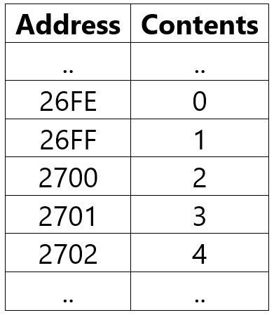
The contents of stack pointer (SP), program counter (PC) and (HL) are 2700H, 2100H and 0000H respectively. When the following sequence of instructions are executed,
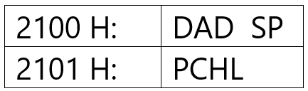
The contents of (SP) and (PC) at the end of execution will be
Explanation Locked!
Unlock this branch to view the explanation, track, bookmark and more.
Sign in to UnlockWhich one of the following statements regarding the INT (interrupt) and the BRQ (bus request) pins in a CPU is true?
Explanation Locked!
Unlock this branch to view the explanation, track, bookmark and more.
Sign in to UnlockThe associated figure shows the two types of rotate right instructions R1, R2 available in a microprocessor where Reg is a 8-bit register and C is the carry bit. The rotate left instructions L1 and L2 are similar except that C now links the most significant bit of Reg instead of the least significant one.

Suppose Reg contains the 2's complement number 11010110. If this number is divided by 2 the answer should be
Explanation Locked!
Unlock this branch to view the explanation, track, bookmark and more.
Sign in to UnlockThe associated figure shows the two types of rotate right instructions R1, R2 available in a microprocessor where Reg is a 8-bit register and C is the carry bit. The rotate left instructions L1 and L2 are similar except that C now links the most significant bit of Reg instead of the least significant one.
Such a division can be correctly performed by the following set of operations
Explanation Locked!
Unlock this branch to view the explanation, track, bookmark and more.
Sign in to UnlockA software delay subroutine is written as given below:
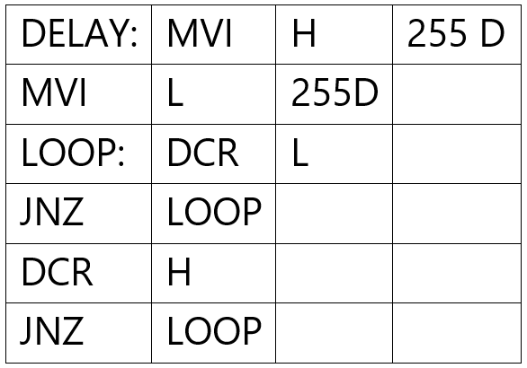
How many times DCR L instruction will be executed?
Explanation Locked!
Unlock this branch to view the explanation, track, bookmark and more.
Sign in to UnlockIn an 8085 microprocessor based system, it is desired to increment the contents of memory location whose address is available in (D, E) register pair and store the result in same location. The sequence of instructions is
Explanation Locked!
Unlock this branch to view the explanation, track, bookmark and more.
Sign in to UnlockThe 8085 assembly language instruction that stores the contents of H and L registers into the memory locations 2050H and 2051H, respectively, is:
Explanation Locked!
Unlock this branch to view the explanation, track, bookmark and more.
Sign in to UnlockIf the following program is executed in a microprocessor, the number of instruction cycles it will take from START TO HALT is
START MVI A, 14 H : Move 14 H to register A
SHIFT RLC : Rotate left without carry
JNZ SHIFT : Jump on non-zero to
SHIFT
HALT
Explanation Locked!
Unlock this branch to view the explanation, track, bookmark and more.
Sign in to UnlockWhen a program is being executed in an 8085 microprocessor, its Program Counter contains
Explanation Locked!
Unlock this branch to view the explanation, track, bookmark and more.
Sign in to UnlockA memory system has a total of 8 memory chips, each with 12 address lines and 4 data lines. The total size of the memory system is
Explanation Locked!
Unlock this branch to view the explanation, track, bookmark and more.
Sign in to UnlockThe following program is written for an 8085 microprocessor to add two bytes located at memory addresses 1FFE and 1FFF
LXI H, 1FFE
MOV B, M
INR L
MOV A, M
ADD B
INR L
MOV M, A
XOR A
On completion of the execution of the program, the result of addition is
Explanation Locked!
Unlock this branch to view the explanation, track, bookmark and more.
Sign in to UnlockThe logic circuit used to generate the active low chip selects (CS) by an 8085 microprocessor to address a peripheral is shown in Figure. The peripheral will respond to addresses in the range.
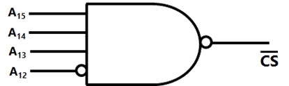
Explanation Locked!
Unlock this branch to view the explanation, track, bookmark and more.
Sign in to UnlockAn intel 8085 processor is executing the program given below.
MVI A, 10H
MVI B, 10H
BACK: NOP
ADD B
RLC
JNC BACK
HLT
The number of times that the operation NOP will be executed is equal to
Explanation Locked!
Unlock this branch to view the explanation, track, bookmark and more.
Sign in to UnlockWhich one of the following is not a vectored interrupt?
Explanation Locked!
Unlock this branch to view the explanation, track, bookmark and more.
Sign in to UnlockIn a microprocessor, the address of the next instruction to be executed, is stored in
Explanation Locked!
Unlock this branch to view the explanation, track, bookmark and more.
Sign in to UnlockThe computer program which converts statements written in high level language to object code is known as
Explanation Locked!
Unlock this branch to view the explanation, track, bookmark and more.
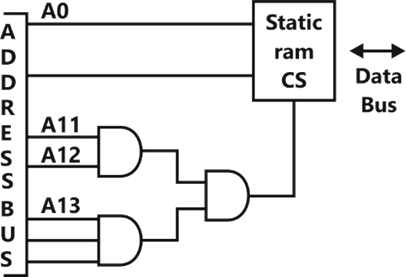
Sign in to UnlockThe range of address for which the memory chip shown in figure, will be selected is_________ to_________
Explanation Locked!
Unlock this branch to view the explanation, track, bookmark and more.
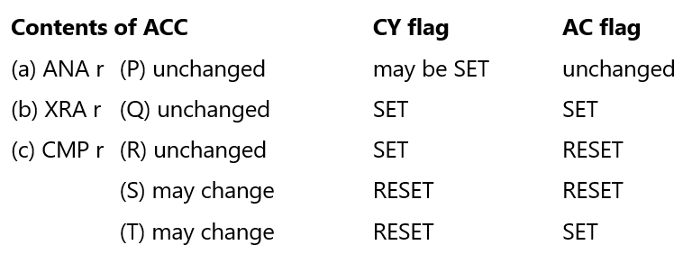
Sign in to UnlockIn a 8085 microprocessor, the following instructions may result in change of accumulator contents and change in status flags. Choose the correct match for each instruction.
Explanation Locked!
Unlock this branch to view the explanation, track, bookmark and more.
Sign in to UnlockIn an 8085 microprocessor, after the execution of XRA A instruction
The carry flag is set

The zero flag is set
The accumulator contents are shifted left by one bit
Explanation Locked!
Unlock this branch to view the explanation, track, bookmark and more.
Sign in to UnlockA subroutine PROG1 written in the 8085 assembly language is given below. At entry to this program, the values of different registers in HEX are. A=05; BC=0000; DE=5472; HL=4528, All the flags are set to 1. Determine the register contents and condition of the zero and carry flags after the execution of the program. (i.e., after executing RET statement). What does the program accomplish?
PROG1 MOV A, E
ADD L
DAA
MOV L, A
MOV A, D
ADC H
DAA
MOV H, A
MVI A, 00H
RAL
RET
Explanation Locked!
Unlock this branch to view the explanation, track, bookmark and more.
Sign in to UnlockThe contents of the accumulator in an 8085 microprocessor is altered after the execution of the instruction.
Explanation Locked!
Unlock this branch to view the explanation, track, bookmark and more.
Sign in to UnlockThe stack pointer of a microprocessor is at A001 At the end of execution of following instructions, the value of stack pointer is _____________
PUSH PSW
X THL
PUSH D
JMP FC70 H
Explanation Locked!
Unlock this branch to view the explanation, track, bookmark and more.
Sign in to UnlockThree devices A, B and C have to be connected to a 8085 microprocessor. Device A has highest priority and device C has the lowest priority. In this context which of the following is correct assignment of interrupt inputs?
Explanation Locked!
Unlock this branch to view the explanation, track, bookmark and more.
Sign in to UnlockIf the HLT instruction of a 8085 microprocessor is executed,
Explanation Locked!
Unlock this branch to view the explanation, track, bookmark and more.
Sign in to Unlock